The Carrier Density Calculator is a crucial tool in semiconductor physics, utilized to determine the concentration of charge carriers—specifically electrons and holes—in different types of semiconductors. This calculation is vital for engineers and researchers who are involved in designing and optimizing semiconductor devices such as diodes, transistors, and integrated circuits. Understanding carrier density is essential for evaluating the electrical properties of materials, predicting their behavior under varying conditions, and ensuring effective performance in various applications.
The calculator differentiates between intrinsic and extrinsic semiconductors, reflecting the unique properties of each type. By accurately calculating carrier densities, users can make informed decisions regarding material selection and device design, which can greatly influence the performance of electronic components.
Formula of Carrier Density Calculator
For Intrinsic Semiconductors
For intrinsic semiconductors, the electron and hole carrier densities are equal and represented as n_i, calculated using the formula:
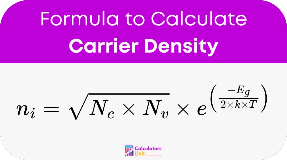
where:
- n_i = Intrinsic carrier density (in cm⁻³)
- N_c = Effective density of states in the conduction band (in cm⁻³)
- N_v = Effective density of states in the valence band (in cm⁻³)
- E_g = Energy band gap (in electron volts, eV)
- k = Boltzmann constant (8.617 × 10⁻⁵ eV/K)
- T = Temperature (in Kelvin, K)
For Extrinsic Semiconductors
In extrinsic (doped) semiconductors, the carrier density for electrons n in n-type and holes p in p-type semiconductors is approximated as follows:
For n-type: n ≈ N_d
For p-type: p ≈ N_a
where:
- n = Electron density (in cm⁻³)
- p = Hole density (in cm⁻³)
- N_d = Donor concentration for n-type material (in cm⁻³)
- N_a = Acceptor concentration for p-type material (in cm⁻³)
General Terms Table
The following table includes commonly searched terms related to carrier density, providing quick references to relevant terminology:
| Term | Definition |
|---|---|
| Carrier Density | The concentration of charge carriers (electrons and holes) in a semiconductor material (in cm⁻³). |
| Intrinsic Semiconductor | A pure semiconductor without any significant dopants, where carrier density is determined by thermal generation. |
| Extrinsic Semiconductor | A semiconductor that has been intentionally doped with impurities to modify its electrical properties. |
| Effective Density of States | A measure of the number of available states for electrons in the conduction and valence bands (in cm⁻³). |
| Energy Band Gap | The energy difference between the conduction band and the valence band (in electron volts, eV). |
| Donor Concentration | The concentration of atoms that donate free electrons in n-type semiconductors (in cm⁻³). |
| Acceptor Concentration | The concentration of atoms that accept electrons in p-type semiconductors (in cm⁻³). |
Example of Carrier Density Calculator
Suppose you are calculating the intrinsic carrier density for a silicon semiconductor at room temperature (approximately 300 K). The effective density of states in the conduction band (N_c) is approximately 1.08 × 10¹⁹ cm⁻³, and in the valence band (N_v) it is approximately 6.00 × 10¹⁸ cm⁻³. The energy band gap (E_g) for silicon is about 1.12 eV.
Using the formula for intrinsic carrier density:
- Calculate n_i:
n_i = √(N_c × N_v) × e^(-E_g / (2 × k × T))
- First, calculate √(N_c × N_v):
√(N_c × N_v) = √(1.08 × 10¹⁹ × 6.00 × 10¹⁸) = √(6.48 × 10³⁷) ≈ 8.05 × 10¹⁸ cm⁻³
- Now, calculate e^(-E_g / (2 × k × T)):
k = 8.617 × 10⁻⁵ eV/K
E_g / (2 × k × T) = 1.12 eV / (2 × 8.617 × 10⁻⁵ eV/K × 300 K) ≈ 21.77
e^(-21.77) ≈ 1.05 × 10⁻⁹
Finally,
n_i ≈ 8.05 × 10¹⁸ cm⁻³ × 1.05 × 10⁻⁹ ≈ 8.45 × 10⁹ cm⁻³
Thus, the intrinsic carrier density of silicon at room temperature is approximately 8.45 × 10⁹ cm⁻³.
Most Common FAQs
Carrier density refers to the concentration of charge carriers (electrons and holes) within a semiconductor material. It is essential for determining the electrical properties of the material and plays a critical role in the performance of semiconductor devices. Understanding carrier density helps in optimizing the design of electronic components such as transistors and diodes.
Carrier density is temperature-dependent. As the temperature increases, more charge carriers are thermally generated, leading to an increase in carrier density in intrinsic semiconductors. Conversely, in extrinsic semiconductors, the effect of temperature can influence the behavior of dopants, thereby affecting the overall carrier concentration.
Yes, the Carrier Density Calculator can be used for both intrinsic and extrinsic semiconductors. The calculations differ slightly depending on the type of semiconductor, but the calculator can accommodate both scenarios to provide accurate results.