The Die Per Wafer Calculator is a crucial tool used in semiconductor manufacturing to estimate the number of individual dies (chips) that can be produced from a single silicon wafer. This calculation helps optimize wafer utilization, reduce manufacturing costs, and improve yield 效率 in the chip fabrication process. By considering wafer size, die dimensions, and edge losses, this calculator provides an accurate estimate of chip production per wafer.
Formula of Die Per Wafer Calculator
The number of dies per wafer can be calculated using the following formula:
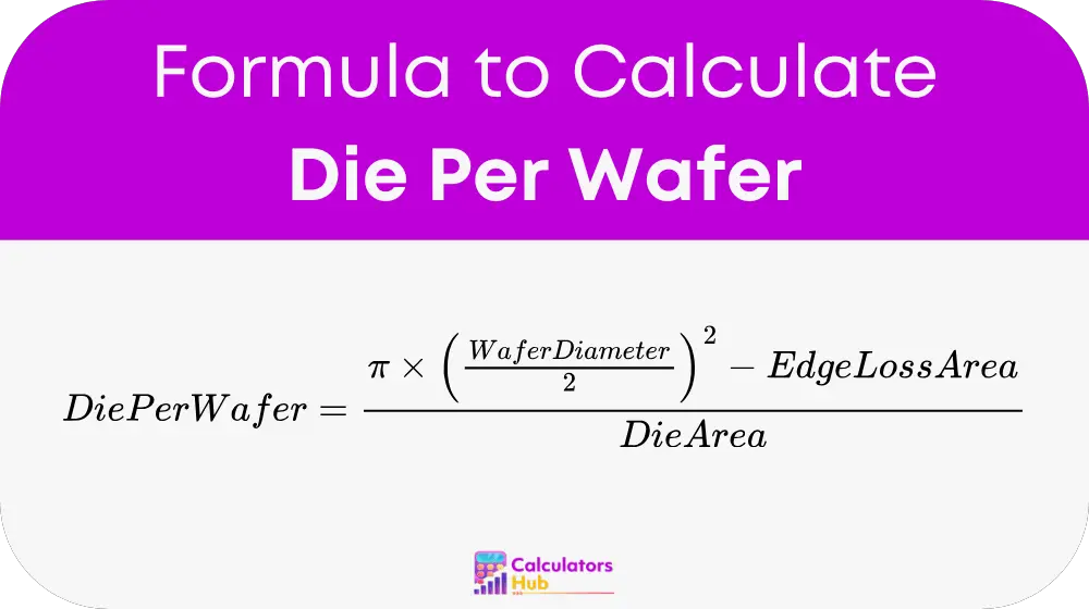
其中:
- 晶圆直径 is the total diameter of the silicon wafer, typically measured in millimeters (mm).
- Edge Loss Area is the unusable portion near the wafer’s edge due to process constraints.
- 模具区 is the area occupied by an individual die, calculated as:Die Area = Die Length × Die Width
This formula provides an estimation of the number of dies that can fit on a wafer while accounting for physical and process limitations.
Die Per Wafer Reference Table
Below is a reference table showing the approximate number of dies per wafer for different wafer sizes and die dimensions:
| Wafer Diameter (mm) | Die Size (mm) | Edge Loss Area (mm^2) | Estimated Dies Per Wafer |
|---|---|---|---|
| 150 | 5 x 5 | 100 | 1800 |
| 200 | 10 x 10 | 150 | 3100 |
| 300 | 15 x 15 | 200 | 6500 |
| 450 | 20 x 20 | 300 | 12500 |
These values provide a general reference for estimating wafer yield in semiconductor fabrication.
Example of Die Per Wafer Calculator
Assume a semiconductor manufacturer is using a 300 mm wafer to produce chips with a die size of 10 mm x 10 mm and an edge loss area of 200mm². The number of dies per wafer can be calculated as follows:
- Calculate the wafer area: Wafer Area = Pi × (300 / 2)^2 Wafer Area = 3.1416 × (150)^2 Wafer Area = 70685 mm²
- Subtract the edge loss area: Usable Area = 70685 - 200 Usable Area = 70485 mm²
- Calculate the number of dies: Die Area = 10 × 10 = 100 mm² Dies Per Wafer = 70485 / 100 Dies Per Wafer ≈ 705
因此,大约 705 人死亡 can be fabricate from a 300 mm wafer using the given parameters.
最常见的常见问题解答
Calculating dies per wafer helps semiconductor manufacturers optimize production efficiency, reduce costs, and improve yield predictions. It also ensures accurate pricing and manufacturing scalability.
Edge loss accounts for the portion of the wafer that cannot be use due to process constraints, such as dicing and handling margins. The larger the edge loss, the fewer usable dies per wafer.
Yes, the die per wafer calculation applies to most semiconductor manufacturing processes, including CMOS, MEMS, and ASIC fabrication, provide the die layout and wafer processing constraints are account for.